- 您现在的位置:买卖IC网 > Sheet目录3832 > PIC16F876A-I/ML (Microchip Technology)IC MCU FLASH 8KX14 A/D 28QFN
PIC16F87XA
DS39582B-page 124
2003 Microchip Technology Inc.
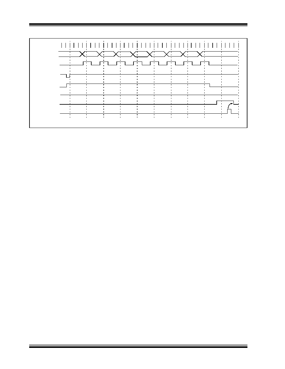
FIGURE 10-11:
SYNCHRONOUS RECEPTION (MASTER MODE, SREN)
10.4
USART Synchronous Slave Mode
Synchronous Slave mode differs from the Master mode
in the fact that the shift clock is supplied externally at
the RC6/TX/CK pin (instead of being supplied internally
in Master mode). This allows the device to transfer or
receive data while in Sleep mode. Slave mode is
entered by clearing bit, CSRC (TXSTA<7>).
10.4.1
USART SYNCHRONOUS SLAVE
TRANSMIT
The operation of the Synchronous Master and Slave
modes is identical, except in the case of the Sleep mode.
If two words are written to the TXREG and then the
SLEEP
instruction is executed, the following will occur:
a)
The first word will immediately transfer to the
TSR register and transmit.
b)
The second word will remain in TXREG register.
c)
Flag bit TXIF will not be set.
d)
When the first word has been shifted out of TSR,
the TXREG register will transfer the second word
to the TSR and flag bit TXIF will now be set.
e)
If enable bit TXIE is set, the interrupt will wake
the chip from Sleep and if the global interrupt is
enabled, the program will branch to the interrupt
vector (0004h).
When setting up a Synchronous Slave Transmission,
follow these steps:
1.
Enable the synchronous slave serial port by set-
ting bits SYNC and SPEN and clearing bit
CSRC.
2.
Clear bits CREN and SREN.
3.
If interrupts are desired, then set enable bit
TXIE.
4.
If 9-bit transmission is desired, then set bit TX9.
5.
Enable the transmission by setting enable bit
TXEN.
6.
If 9-bit transmission is selected, the ninth bit
should be loaded in bit TX9D.
7.
Start transmission by loading data to the TXREG
register.
8.
If using interrupts, ensure that GIE and PEIE
(bits 7 and 6) of the INTCON register are set.
CREN bit
RC7/RX/DT
RC6/TX/CK
Write to
bit SREN
SREN bit
RCIF bit
(Interrupt)
Read
RXREG
Note: Timing diagram demonstrates Sync Master mode with bit SREN = 1 and bit BRG = 0.
Q3 Q4 Q1 Q2 Q3 Q4 Q1 Q2 Q3 Q4
Q2
Q1 Q2 Q3 Q4Q1 Q2 Q3 Q4 Q1 Q2 Q3 Q4Q1 Q2 Q3 Q4 Q1 Q2 Q3 Q4Q1 Q2 Q3 Q4 Q1 Q2 Q3 Q4
‘0’
bit 0
bit 1
bit 2
bit 3
bit 4
bit 5
bit 6
bit 7
‘0’
Q1 Q2 Q3 Q4
pin
发布紧急采购,3分钟左右您将得到回复。
相关PDF资料
PIC16F876A-I/SO
IC MCU FLASH 8KX14 EE 28SOIC
PIC16F876A-I/SP
IC MCU FLASH 8KX14 EE 28DIP
AT87C51RD2-3CSUM
IC 8051 MCU 64K OTP 40MHZ 40DIP
DSPIC33FJ64MC802-I/SO
IC DSPIC MCU/DSP 64K 28-SOIC
DSPIC33FJ64GP802-I/MM
IC DSPIC MCU/DSP 64K 28-QFN
AT87C51RD2-3CSUL
IC 8051 MCU 64K OTP 30MHZ 40DIP
PIC18F2431-I/SP
IC PIC MCU FLASH 8KX16 28DIP
AT87C51RC2-SLSUM
IC 8051 MCU 32K OTP 40MHZ 44PLCC
相关代理商/技术参数
PIC16F876A-I/ML
制造商:Microchip Technology Inc 功能描述:IC 8BIT FLASH MCU SMD 制造商:Microchip Technology Inc 功能描述:IC, 8BIT FLASH MCU, SMD
PIC16F876A-I/MLG
功能描述:8位微控制器 -MCU 14KB 368 RAM 22 I/O Lead Free Package RoHS:否 制造商:Silicon Labs 核心:8051 处理器系列:C8051F39x 数据总线宽度:8 bit 最大时钟频率:50 MHz 程序存储器大小:16 KB 数据 RAM 大小:1 KB 片上 ADC:Yes 工作电源电压:1.8 V to 3.6 V 工作温度范围:- 40 C to + 105 C 封装 / 箱体:QFN-20 安装风格:SMD/SMT
PIC16F876A-I/SO
功能描述:8位微控制器 -MCU 14KB 368 RAM 22 I/O RoHS:否 制造商:Silicon Labs 核心:8051 处理器系列:C8051F39x 数据总线宽度:8 bit 最大时钟频率:50 MHz 程序存储器大小:16 KB 数据 RAM 大小:1 KB 片上 ADC:Yes 工作电源电压:1.8 V to 3.6 V 工作温度范围:- 40 C to + 105 C 封装 / 箱体:QFN-20 安装风格:SMD/SMT
PIC16F876A-I/SO
制造商:Microchip Technology Inc 功能描述:8BIT FLASH MCU SMD 16F876 SOIC28
PIC16F876A-I/SOE3
制造商:Microchip Technology Inc 功能描述:8-BIT, FLASH, 20 MHz, RISC MICROCONTROLLER, 28 Pin Plastic SMT
PIC16F876A-I/SOG
功能描述:8位微控制器 -MCU 14KB 368 RAM 22 I/O RoHS:否 制造商:Silicon Labs 核心:8051 处理器系列:C8051F39x 数据总线宽度:8 bit 最大时钟频率:50 MHz 程序存储器大小:16 KB 数据 RAM 大小:1 KB 片上 ADC:Yes 工作电源电压:1.8 V to 3.6 V 工作温度范围:- 40 C to + 105 C 封装 / 箱体:QFN-20 安装风格:SMD/SMT
PIC16F876A-I/SP
功能描述:8位微控制器 -MCU 14KB 368 RAM 22 I/O RoHS:否 制造商:Silicon Labs 核心:8051 处理器系列:C8051F39x 数据总线宽度:8 bit 最大时钟频率:50 MHz 程序存储器大小:16 KB 数据 RAM 大小:1 KB 片上 ADC:Yes 工作电源电压:1.8 V to 3.6 V 工作温度范围:- 40 C to + 105 C 封装 / 箱体:QFN-20 安装风格:SMD/SMT
PIC16F876A-I/SP
制造商:Microchip Technology Inc 功能描述:IC 8BIT FLASH MCU 16F876 SDIL28